
Materials
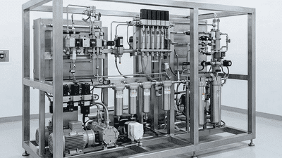
Precursor Demand in ALD and CVD: The Korean Supplier Dominance
A semiconductor’s most important materials are not always visible in the finished device. Some arrive at the factory inside specialized containers, enter a deposition chamber as vapor, and disappear into films only a few nanometers thick. These precursors help form the insulating layers, electrodes, barriers, and other structures that allow modern chips to operate.

Wet Chemicals G5 Purity: The Domestic Qualification Breakthrough
A semiconductor fabrication plant can install advanced equipment, secure high-quality silicon wafers, and develop sophisticated process recipes, yet still lose performance to contamination carried by an ordinary-looking liquid. Sulfuric acid, hydrogen peroxide, hydrofluoric acid, and ammonia solutions appear unremarkable beside a lithography scanner. Inside the fab, however, their cleanliness can influence whether a carefully engineered surface survives the next manufacturing step.

CMP Slurry Advances: Dinglong’s Cerium Oxide and TSV Polishing Wins
The semiconductor supply chain has a habit of hiding its most consequential dependencies behind its least glamorous materials. Advanced lithography attracts headlines. AI accelerators attract capital. Yet before a chip can become either a technological breakthrough or a commercial success, it needs a wafer—and most mainstream silicon wafer production depends on growing a single crystal inside a quartz crucible.

Electronic Specialty Gas Demand from Advanced Nodes: The Localization Acceleration
Semiconductor manufacturing is often described through its most visible assets: lithography machines, cleanrooms, silicon wafers, and increasingly expensive fabrication plants. Yet some of the materials that determine whether those investments produce usable chips arrive through pipes and cylinders. Electronic specialty gases belong to this less visible but strategically important layer of the industry.
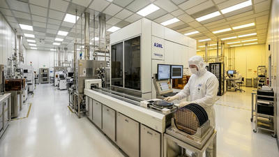
Photoresist Pricing: Shin-Etsu and JSR’s China Strategy Shift
Photoresist pricing has become a revealing lens through which to examine the changing relationship between Japanese materials suppliers and China’s semiconductor industry. For a wafer fab, photoresist is a recurring procurement item. For a process engineer, it is a carefully qualified component of a manufacturing recipe. For a supplier such as Shin-Etsu Chemical or JSR, it represents a combination of chemical expertise, customer integration, and commercial leverage.

Semiconductor Material Hidden Champions: The Small-Cap Opportunity Map
The semiconductor market rewards visible products: accelerators, memory, leading-edge manufacturing, and the equipment that makes them possible. Far less visible are the materials that allow those operations to run consistently. A wafer, photoresist formulation, specialty gas, or sputtering target may attract little attention until its quality or availability becomes a production problem.
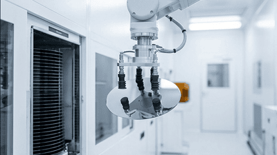
Silicon Wafer Shipment Area Growth: The 2026 Recovery Trajectory
The silicon wafer market is recovering in 2026, but the recovery is neither uniform nor adequately explained by the artificial intelligence investment boom alone. Shipment area is increasing, advanced applications remain the strongest demand engine, and industrial and automotive markets are showing signs of improvement. Yet rising volumes do not automatically imply stronger pricing, fully utilized factories, or an equally healthy outlook across wafer categories.
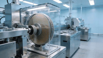
Wafer Edge Polishing Equipment: The SOI Substrate Demand Driver
The center of a semiconductor wafer receives most of the attention. That is where engineers measure film thickness, pattern devices, and evaluate electrical performance. The edge looks less productive: a narrow perimeter that cannot accommodate complete dies and often sits outside the usable processing area.

Advanced Packaging Material Demand: Underfill and TIM Localization
A large AI package can contain exceptional silicon and still fail because a relatively inexpensive material does not behave as expected. An underfill that leaves voids can compromise interconnect reliability. A thermal interface material that loses contact can turn an acceptable cooling design into a temperature problem.
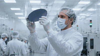
2026 Global Wafer Shipment Area YoY Growth Forecasts: Divergence and Consensus
As the semiconductor industry moves through 2026, expectations for global wafer shipping area growth sit at the core of many strategic decisions. Year‑on‑year (YoY) wafer area forecasts influence how wafer manufacturers plan capacity, how fabs schedule expansions and technology migrations, and how equipment and materials suppliers shape their own production plans. Yet the forecasts themselves are far from uniform. Different institutions—industry bodies, market research firms, banks, and corporate strategists—offer projections that diverge meaningfully in magnitude and composition, even when they point in broadly similar directions.