
Inspection and Metrology Tools: The Yield Improvement Lever in 3nm
A 3nm manufacturing process can be technically impressive and commercially disappointing at the same time. The difference often lies in how consistently it produces usable devices. Expensive production equipment establishes the capability to manufacture advanced structures; inspection and metrology help determine whether that capability becomes repeatable, economical output.
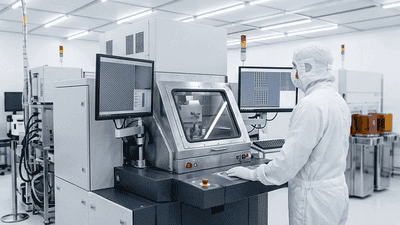
Their role is increasingly strategic. As process tolerances tighten, engineers need to identify defects, measure variation, and connect those observations to manufacturing decisions before additional processing makes a problem more expensive.
The essential concept is feedback. Inspection and metrology do not directly repair a transistor or eliminate a particle. They reveal information that allows engineers and control systems to adjust processes, investigate equipment, and prevent unsuitable material from continuing through production. At 3nm, the quality and speed of that information can influence the entire yield-learning cycle.
What “3nm” Does—and Does Not—Tell Us
The 3nm label identifies a technology generation, not a universal physical dimension shared by every feature on a chip. Different manufacturers can implement different structures and process choices within that generation.
This matters when discussing measurement requirements. There is no single “3nm inspection setting” that applies uniformly across all layers, devices, and manufacturers.
The relevant questions concern the actual structures being fabricated: which dimensions are critical, where alignment matters, what defects can cause electrical failure, and which variations remain acceptable.
For equipment suppliers, that creates application-specific opportunities. For fabs, it means process control must be designed around the manufacturing flow rather than around a node label. The objective is not measurement for its own sake, but information that protects the intended device performance.
Inspection Finds Problems; Metrology Quantifies Conditions
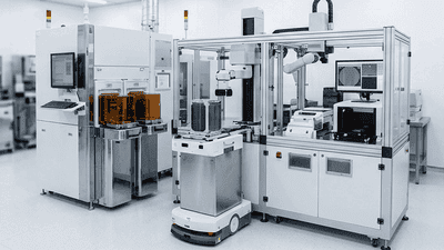
Inspection and metrology are closely related, but they serve different primary purposes. Inspection searches for anomalies such as particles, pattern defects, and unexpected structural conditions. Metrology measures characteristics such as dimensions, film thickness, and alignment.
The distinction becomes useful when diagnosing yield loss. Inspection may show where a defect appears, while metrology helps determine whether a process parameter has moved outside its acceptable range.
Neither approach alone provides a complete picture. A wafer can contain an isolated defect despite acceptable average measurements, or show systematic dimensional drift without a conspicuous particle.
Combining measurements and defect observations helps engineers distinguish random events from recurring process problems. That connection is what turns separate equipment outputs into a manufacturing control strategy.
Yield Improvement Begins Before Final Electrical Test
Final electrical test establishes whether devices meet the required specifications, but it occurs after substantial manufacturing value has already been added.
If a problem originated much earlier, waiting until final test can leave engineers investigating many possible causes. By then, affected material may have passed through numerous additional steps.
Inline inspection and measurement create earlier opportunities to detect abnormal conditions. A customer can investigate a chamber, adjust a process, or hold material while the evidence is still closely connected to the originating operation.
From a factory manager’s perspective, this improves more than yield. It can reduce uncertainty, limit the amount of material exposed to an excursion, and shorten the time needed to restore stable production. The benefit depends on prompt interpretation and action—not simply on collecting data.
Critical Dimensions Need More Than an Average
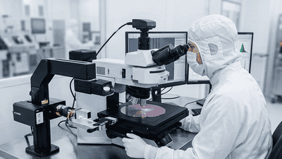
Critical-dimension measurements examine geometries that influence device behavior. At advanced nodes, engineers must consider variation across a wafer, between wafers, and over time.
An acceptable average can conceal an unacceptable distribution. Local regions may behave differently, or a process may gradually drift while its overall mean remains deceptively reassuring.
This creates a sampling challenge. Measurements must be representative enough to reveal relevant variation without consuming excessive production time.
For a process engineer, the practical question is whether the measurement plan can detect the failure mechanism being investigated. More measurements are not automatically better if they repeat information from low-risk locations while missing the regions that matter.
Overlay Connects Individual Layers into a Working Device
Semiconductor manufacturing builds structures through multiple patterning and processing stages. Overlay metrology examines the alignment relationship between layers.
That relationship matters because correctly formed features can still fail to connect or remain separated as intended if their relative positions are wrong.
Engineers also need to consider the combined effect of dimensional variation and placement. Measuring alignment alone does not establish that every feature edge occupies the desired location.
The yield lever is therefore a coordinated view of geometry. Lithography, deposition, and etching can influence the final result in different ways. Effective process control connects those contributions rather than assuming that one measurement fully describes the finished structure.
EUV Patterning Creates a Distinct Inspection Challenge
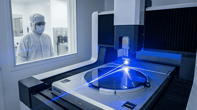
Extreme ultraviolet lithography enables demanding patterning, but successful exposure does not remove the need to evaluate what was actually formed.
Engineers must distinguish systematic patterning behavior from isolated failures. Some problems can recur in identifiable locations or conditions; others are less predictable and require a different inspection strategy.
This increases the importance of connecting defect observations with design context, process settings, and subsequent results. A defect count becomes more useful when engineers understand which defects are likely to affect device function.
The commercial opportunity for inspection suppliers is not simply detecting smaller objects. It is helping customers identify consequential failures quickly enough to improve the process and avoid repeating them.
Optical Tools Provide Broad Coverage and Speed
Optical inspection and metrology play a major role because they can support production-oriented coverage and measurement throughput. Different optical approaches address patterns, films, surfaces, and other characteristics.
Their value depends on the contrast or signal associated with the feature being examined. A defect’s physical size is important, but it is not the only factor determining detectability.
This is why simplistic comparisons between optical wavelength and minimum defect size can misrepresent what a system can accomplish. The measurement method, application, and analysis all matter.
For fabs, optical tools often provide a practical route to broad monitoring. Their results can guide further investigation, helping more specialized techniques concentrate on locations where additional detail is most valuable.
Electron-Beam Tools Add Detail, with a Productivity Trade-Off
Electron-beam techniques can provide detailed examination of selected structures and defects. They are valuable when the required information is not adequately captured by another method.
However, detailed examination has an operating cost. Coverage, acquisition time, and production throughput must be considered alongside resolution and sensitivity.
The sensible strategy is usually complementary rather than absolute. One technique identifies areas of concern, another characterizes them more closely, and the combined evidence supports a decision.
For equipment investors, this means that technical capability alone does not determine adoption. Customers evaluate how effectively a system fits the inspection workflow and whether its additional information justifies the time and cost required to obtain it.
Three-Dimensional Structures Require Multiple Perspectives
As structures become more complex, a top-down image may not reveal every characteristic relevant to performance. Engineers may need information about profiles, films, interfaces, or features that are difficult to observe directly.
Different techniques can address different parts of that problem. Some measurements infer structural properties from a model, while others provide more direct observations of selected locations.
Model quality becomes important whenever the result depends on assumptions about the structure. A precise-looking number is not necessarily accurate if the underlying model is inappropriate.
This creates demand for complementary measurement and calibration. The objective is to build confidence in the process information, not to assume that one instrument can comprehensively describe every aspect of a complex device.
Sampling Is a Manufacturing Decision
Inspecting everything at maximum sensitivity would consume time and resources that production cannot always justify. Inspecting too little risks allowing problems to propagate.
A good sampling plan reflects process risk, historical behavior, equipment changes, and the consequences of missing a defect. It can evolve as a process matures.
During development or after a significant change, additional coverage may be justified. During stable production, a different balance may provide adequate protection with less measurement effort.
From a factory perspective, this is an optimization problem. The goal is not maximum inspection intensity everywhere. It is enough relevant information, gathered at the right points, to maintain control and respond when conditions change.
Data Integration Determines the Value of the Tools
A fab can own excellent instruments and still struggle to improve yield if their outputs remain disconnected. Defect maps, dimensional measurements, equipment histories, and electrical results become more informative when they can be analyzed together.
That integration helps engineers identify patterns: a recurring chamber signature, a location-specific issue, or a change associated with maintenance or a new material lot.
Automation and analytical models can assist, but their conclusions require validation. Historical correlations can weaken when the process, equipment, or product changes.
The most useful software does not merely summarize more data. It helps engineers prioritize evidence, trace possible causes, and decide what action is appropriate. Faster analysis matters when it shortens the path from detection to correction.
The Back-End Must Preserve the Front-End Gain
A high-quality 3nm die can still be lost during packaging. Bonding, handling, interconnection, and assembly create additional opportunities for defects and variation.
Advanced packaging therefore needs its own inspection and metrology strategy. Alignment, dimensions, warpage, and internal structural conditions can matter, depending on the package architecture.
Different techniques address different questions. For example, automated X-ray metrology can measure selected bump and package characteristics that are not adequately described by surface inspection alone.
The connection to front-end yield is economic rather than identical in scale. Packaging tools do not need to reproduce transistor-level measurements to protect the value of advanced dies. They need to control the risks introduced by the assembly process.
The Business Case Is Cost per Acceptable Device
Inspection and metrology increase manufacturing cost, so their value must be evaluated against the losses they help prevent and the improvements they enable.
A tool can justify itself by accelerating a yield ramp, limiting an excursion, reducing unnecessary rework, or supporting a more stable process. The relevant benefit depends on the application.
There is no universal percentage by which inspection spending raises 3nm yield. Results depend on the starting process, failure mechanisms, implementation, and response.
For a financial analyst, the useful denominator is acceptable output. A higher process-control budget can be economically attractive if it lowers the overall cost of producing usable devices. Equally, more spending is not inherently better if the additional information does not change manufacturing decisions.
What Equipment Investors Should Watch
The strongest indicators connect technical capability with sustained customer use.
- Look for qualified applications rather than specifications alone.
- Distinguish development tools from systems deployed in recurring production.
- Track repeat orders and expansion into additional process steps.
- Assess throughput, useful sensitivity, and false-positive management together.
- Examine software integration and field-support requirements.
- Separate front-end measurement demand from packaging-specific opportunities.
These factors help explain why suppliers can experience different outcomes despite serving the same technology generation. Customer value depends on solving a relevant control problem, not simply on attaching “3nm” to a product description.
The Lever Works Only When Information Becomes Action
Inspection and metrology are essential to turning advanced manufacturing capability into reliable production. Their contribution lies in revealing defects, quantifying variation, and shortening the learning cycle.
At 3nm, that role becomes more consequential because manufacturing decisions must be made with tighter tolerances and more accumulated value at risk. The back end then needs to preserve the gains achieved during fabrication.
The lasting advantage belongs to fabs and suppliers that connect measurement with effective action. Better visibility is the beginning. Better controlled production is the result that matters.